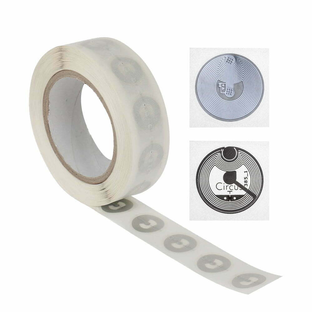
NFC Inlay antennas are typically manufactured using either etched aluminum or copper wire winding processes. While the chip serves as the core component, the physical integrity of the antenna directly determines the sensing distance and the product’s lifespan.
The following are four key dimensions for visual inspection:
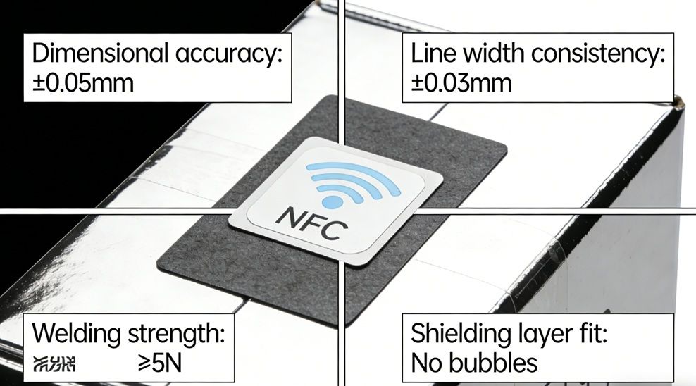
1.Edge Definition and Etching Precision
The edges of a high-quality antenna circuit should be sharp and smooth.
- Inspection Point: Use a 10x magnifying glass to examine the edges of the antenna coil.
- High-Quality Indicators: The circuit edges are crisp and free of burrs, and the spacing between the coil turns is uniform and consistent.
- Warning Signs (Poor Quality): Edges exhibit a sawtooth or splatter-like appearance. This is typically caused by uncontrolled chemical concentrations in the etching solution or an excessively fast etching speed; such defects can easily lead to localized charge accumulation, thereby compromising signal stability.
2.Oxidation and Discoloration
The chemical stability of the antenna surface determines its shelf life within storage environments.
Inspection Point: Examine the surface of the aluminum or copper circuitry for the presence of black spots, white patches, or darkened areas.
High-Quality Indicators: Aluminum antennas exhibit a uniform, silvery-white metallic luster; copper antennas display a bright, vibrant orange-gold hue.
Warning Signs (Poor Quality):
- Black Spots/Mold: Indicates excessive humidity in the production environment or the presence of chemical residues on the surface, which can lead to increased electrical resistance.
- White Powder (on Aluminum): This is a classic sign of aluminum oxidation (specifically aluminum hydroxide), which can result in an open circuit within the antenna.
- Rainbow Patterns: Indicates uneven application of the surface coating/film, which increases the risk of delamination.
3.IC Bonding Area Condition
The junction where the chip connects to the antenna (via bumps or leads) is the most fragile point of the entire inlay.
Inspection Point: Check whether the transparent conductive adhesive (ACP) beneath the chip has excessively overflowed, and verify that the chip is correctly aligned.
High-Quality Indicators: The chip is centrally positioned with uniform pressure marks, and there are no visible traces of black carbonization around the perimeter.
Warning Signs (Poor Quality):
- Chip Misalignment: The chip does not fully cover the antenna’s contact points; this can result in a halved sensing distance or intermittent operational failure.
- Bubbles: The presence of air bubbles within the bonding adhesive poses a risk; upon subsequent exposure to heat, these bubbles may expand and potentially “dislodge” the chip from the antenna.
4.Connection Points and Fracture Risks (Micro-cracks)
Due to the extreme thinness of the inlay, microscopic cracks are prone to forming during the roll-winding process.
Inspection Focus: Pay particular attention to the corners of the antenna coil.
High-Quality Indicators: Corners appear smooth, and the PET substrate shows no visible “whitening” (an indication of creasing).
Warning Signs: The corners exhibit minute cracks or deep indentations resulting from excessive die-cutting pressure. Once the label is applied to a curved surface, these micro-cracks can rapidly propagate, leading to a complete open circuit.
5.Practical QC Recommendations
| Inspection Item | Method | Acceptance Criteria | Remarks |
| Reflectivity | Tilt at a 45° angle under light | Uniform metallic luster; no dark spots | Assess oxidation risk |
| Alignment | Transmitted light observation | Chip and antenna solder points are perfectly superimposed | Assess connection reliability |
| PET Integrity | Tensile Test (Sample Roll) | Substrate shows no delamination or whitening from creases | Assess processing durability |
| Circuit Spacing | Magnified visual inspection | No residual metal bridging between circuit lines | Assess short-circuit risk |
6.Summary
Visual inspection serves as the first line of defense. “Sharp edges, a glossy surface, and centered bonding” constitute the three key visual characteristics of a high-quality inlay. If more than 3% of the inlays within a given batch exhibit any of the aforementioned visual defects, it is recommended to conduct comprehensive electrical performance testing on the entire batch.
For more information,please contact us.